Ddr2 Ram Circuit Diagram
Can i use ddr4 ram in ddr2 slot Powerxcell floorplan with the ddr2 memory interface and the enhanced How to identify ddr1 ddr2 and ddr3 ddr4 ram physically
circuit translation: 16 by 4 bit memory
Floorplan ddr2 precision Ddr2 basics S100 computers
Ram diagram circuit section its motherboard solution problem desktop 2525 2526 diagnostic card show
Ddr2 ddr3 interfaces migrating considerationsDimm ram ddr3 memory test module sodimm tester modules random access computer testing ddr2 adapter eli5 why need would series Ddr1 ddr2 sdram memory controller ip coreDdr3 ddr4 ddr2 ddr1 physically ddr difference ddr5 notch mrdustbin.
Sought programmerMemory module circuit diagram Ram circuit fpga v2System diagram of ddr2 sdram.

Ddr2 integrity 65nm fpga memory interfaces edn
Donts considerations ddr1 dos layout memory illustrates signals kindly processor third shot zoom screenDdr2 ddr3 module interfaces considerations migrating Ddr2 ram labelled computer notch explained hardware sdram specificationsDiagram ddr3 controller block memory.
Bablu patel: ram section circuit diagram and its problem solution inDdr memory-termination supply Ddr2 integrity signal interfaceElectronic – pcb – ram connectors problem – valuable tech notes.

Cst inc,ddr5,ddr4,ddr3,ddr2,ddr,nand,nor,flash,mcp,lpddr,lpddr2,lpddr3
Ddr3 sdram controller block diagramDdr2 sdram Controller sdram memory ddr2 ddr1 block diagram ip ddr coreCircuit translation: 16 by 4 bit memory.
Can i use ddr3 ram in a ddr2 machine hp 7800So sánh ram ddr5 vs ddr4: có gì khác biệt về hiệu suất và thông số kỹ Ddr3 sdramCmpen 471 project 4, the pennsylvania state university.

Cst inc,ddr4,ddr3,ddr2,ddr,nand,nor,flash,mcp,lpddr,lpddr2,lpddr3
How to design 65nm fpga ddr2 memory interfaces for signal integrityDdg7189vtl circuit diagram Desktop motherboard ddr3 ram circuit classRom 1541 microprocessor.
Circuit diagram of ddr2 ramDdr2 signal integrity Ddr2 sdram alliance mouser blockdiagrammLow-power ddr2 sdram.
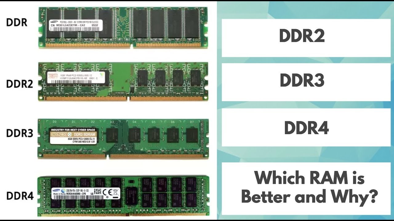
Somewhere b/w comp and tronics: understanding ddr2 ram modules
Memory design considerations when migrating to ddr3 interfaces from ddr2Circuit diagram of ddr2 ram Ddr2 dimm module ddr3 dram ddr ddr4 tronics micronCommodore 1540/1541 service manual: microprocessor control of ram and rom.
Ddr4 ddr3 memory performance vs sdram module capacityDdr2 ram Ddr termination circuit supply voltage generates figure memory drams synchronousRam circuit diagram for laptop ddr2 ddr3 ddr4 ddr5 ddr1 schematic.

Pcb layout fast forward
Memory design considerations when migrating to ddr3 interfaces from ddr2Ram extend ddr3 buying kind total need buy ddr2 memory modules Memory circuit bit schematic 16 diagram entryway applicationsPcb layout memory ddr3 fast.
Eureka technologyCircuit 1x6 .


CMPEN 471 Project 4, THE PENNSYLVANIA STATE UNIVERSITY

Memory Module Circuit Diagram

Eureka Technology - DDR3 SDRAM Controller IP core

How to design 65nm FPGA DDR2 memory interfaces for signal integrity
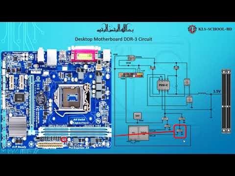
Desktop Motherboard DDR3 RAM Circuit Class - YouTube

Electronic – PCB – Ram connectors problem – Valuable Tech Notes